Their method might change a clinical field reliant on cost-prohibitive innovation.
Scientists at the Georgia Institute of Innovation have actually established a light-based methods of printing nano-sized metal structures that is substantially faster and more affordable than any innovation presently offered. It is a scalable service that might change a clinical field long reliant on innovations that are excessively costly and sluggish. The development has the possible to bring brand-new innovations out of laboratories and into the world.
Benefits of the New Method
Technological advances in numerous fields count on the capability to print metal structures that are nano-sized– a scale numerous times smaller sized than the width of a human hair. Sourabh Saha, assistant teacher in the George W. Woodruff School of Mechanical Engineering, and Jungho Choi, a Ph.D. trainee in Saha’s laboratory, established a method for printing metal nanostructures that is 480 times much faster and 35 times more affordable than the present traditional approach.
Their research study was released in the journal Advanced Products
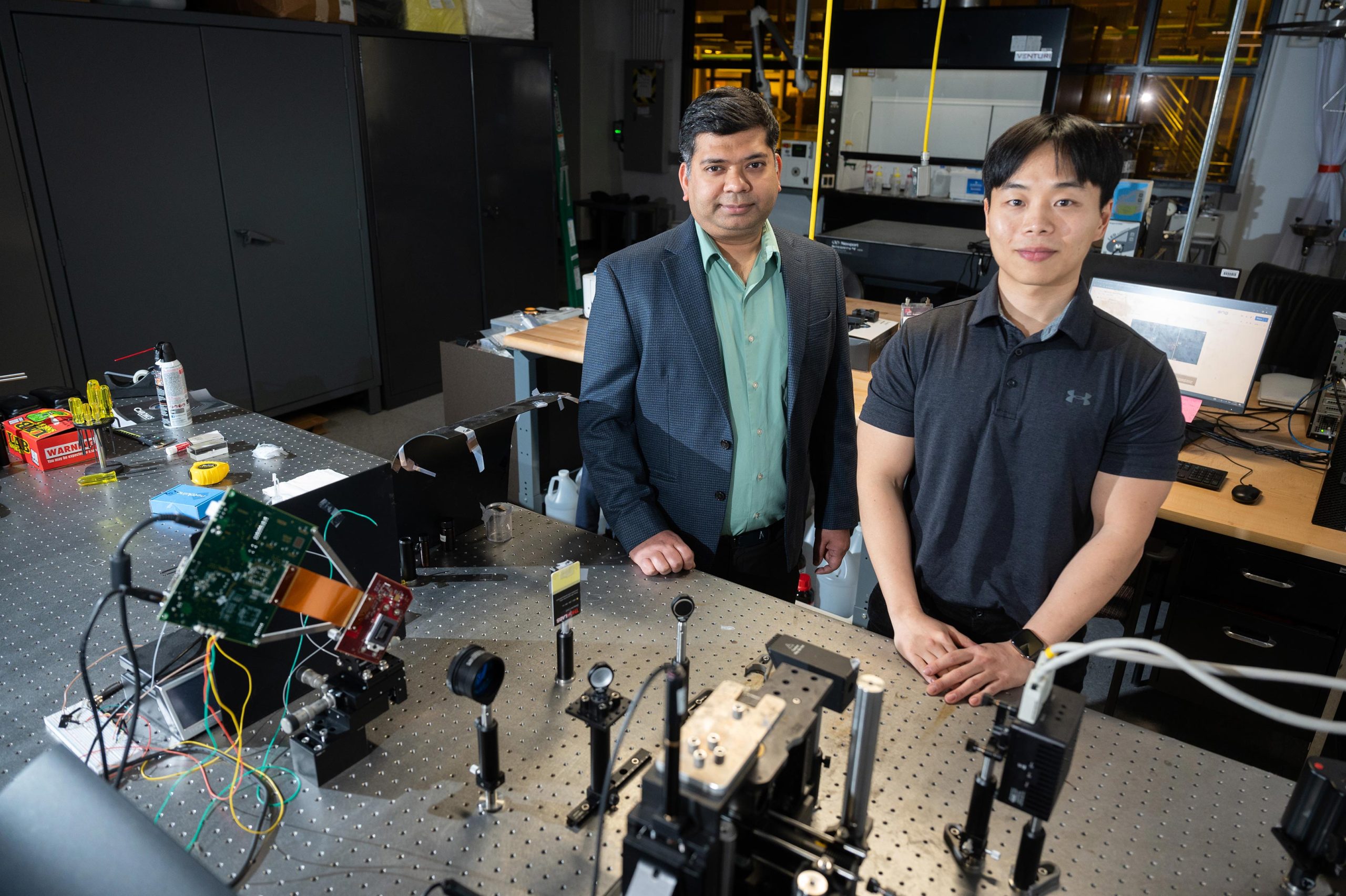
Assistant Teacher Sourabh Saha and Jungho Choi (Ph.D. trainee) in front of their superluminescent light forecast system at Georgia Tech. Credit: Georgia Institute of Innovation
Getting Rid Of Standard Limitations
Printing metal on the nanoscale — a method called nanopatterning– enables the production of special structures with fascinating functions. It is vital for the advancement of numerous innovations, consisting of electronic gadgets, solar power conversion, sensing units, and other systems.
It is normally thought that high-intensity source of lights are needed for nanoscale printing. However this kind of tool, called a femtosecond laser, can cost approximately half a million dollars and is too costly for a lot of research study laboratories and small companies.
” As a clinical neighborhood, we do not have the capability to make sufficient of these nanomaterials rapidly and cost effectively, which is why appealing innovations frequently remain minimal to the laboratory and do not get equated into real-world applications,” Saha stated.
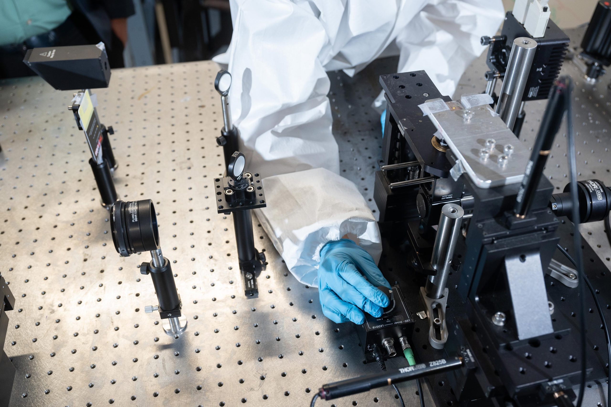
Ph.D. trainee Jungho Choi managing LED brightness levels on the SLP system. Credit: Georgia Institute of Innovation
” The concern we wished to address is, ‘Do we actually require a high-intensity femtosecond laser to print on the nanoscale?’ Our hypothesis was that we do not require that light to get the kind of printing we desire.”
They looked for an affordable, low-intensity light that might be focused in such a way comparable to femtosecond lasers, and selected superluminescent light giving off diodes (SLEDs) for their business accessibility. SLEDs discharge light that is a billion times less extreme than that of femtosecond lasers.
A video of nanoprinting with superluminescent light forecast (SLP). Credit: Georgia Institute of Innovation
Ingenious Printing Innovation
Saha and Choi set out to produce an initial projection-style printing innovation, creating a system that transforms digital images into optical images and shows them on a glass surface area. The system runs like digital projectors however produces images that are more dramatically focused. They leveraged the special homes of the superluminescent light to produce dramatically focused images with very little problems.
They then established a clear ink service comprised of metal salt and included other chemicals to ensure the liquid might soak up light. When light from their forecast system struck the service, it triggered a chain reaction that transformed the salt service into metal. The metal nanoparticles adhered to the surface area of the glass, and the heap of the metal particles produces the nanostructures. Since it is a forecast kind of printing, it can print a whole structure in one go, instead of point by point– making it much quicker.
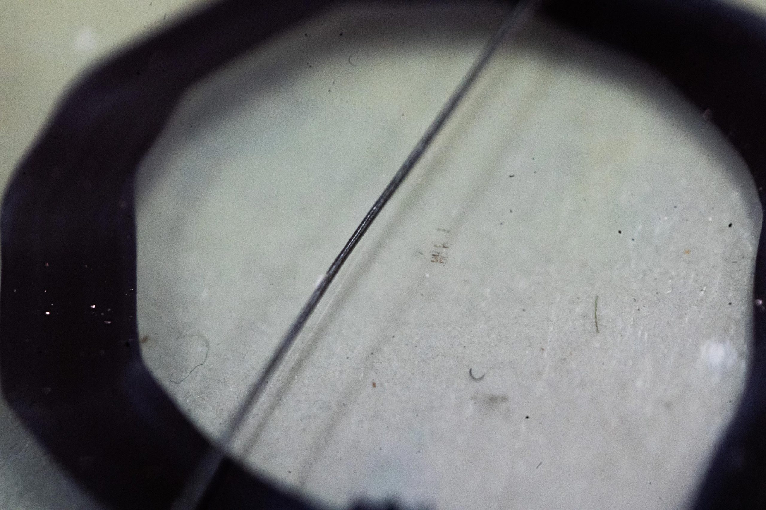
Size contrast in between human hair (~ 100 micrometer density) versus printed silver pad on a glass coverslip. Credit: Georgia Institute of Innovation
After checking the method, they discovered that projection-style nanoscale printing is possible even with low-intensity light, however just if the images are dramatically focused. Saha and Choi think that scientists can easily duplicate their work utilizing commercially offered hardware. Unlike a costly femtosecond laser, the kind of SLED that Saha and Choi utilized in their printer costs about $3,000.
Applications
” At present, just leading universities have access to these costly innovations, and even then, they lie in shared centers and are not constantly offered,” Choi stated. “We wish to equalize the ability of nanoscale 3D printing, and we hope our research study unlocks for higher access to this kind of procedure at a low expense.”
The scientists state their method will be especially helpful for individuals operating in the fields of electronic devices, optics, and plasmonics, which all need a range of complicated metal nanostructures.
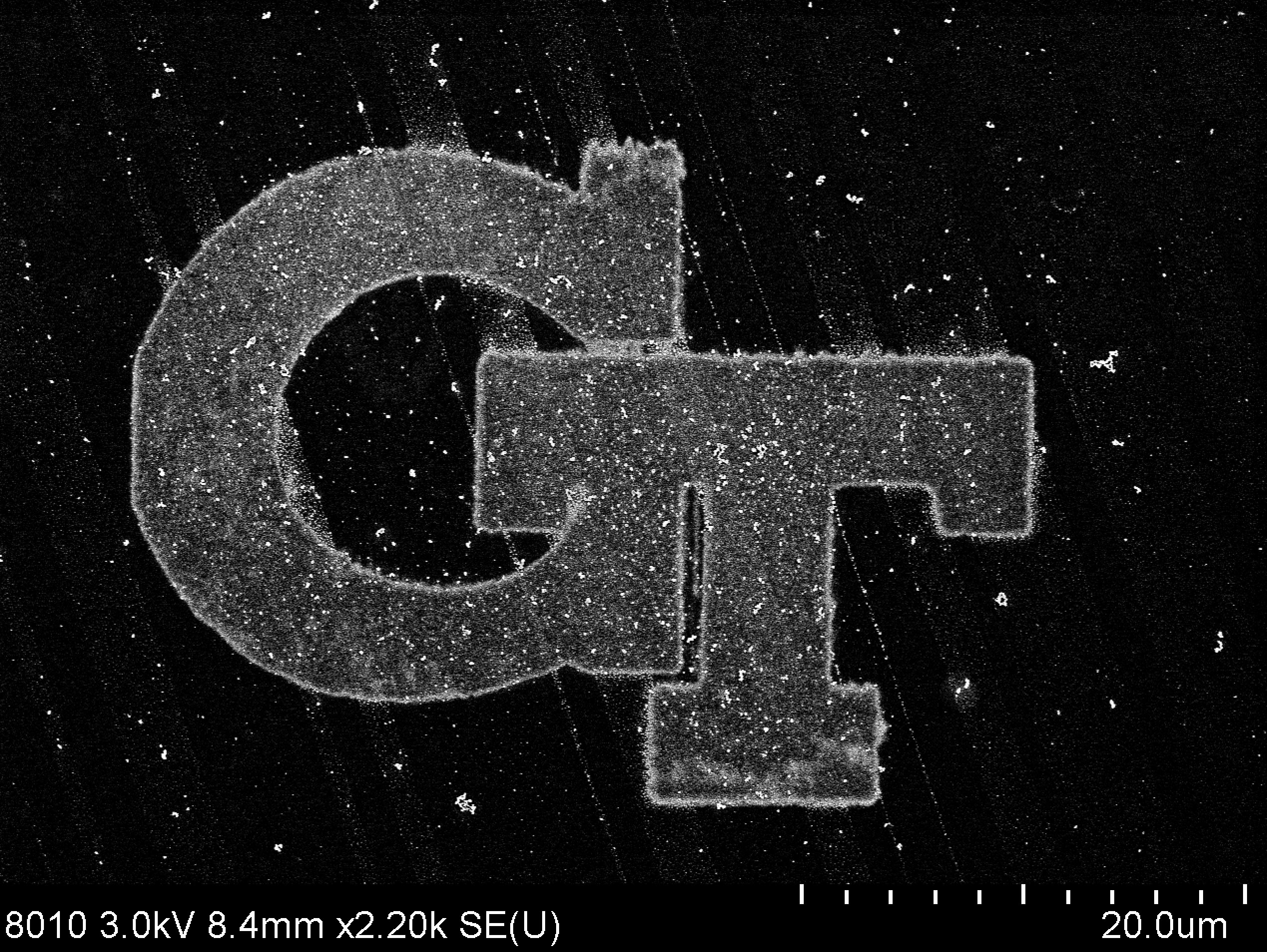
Scanning electron microscopic lense picture of printed silver GT pattern Credit: Georgia Institute of Innovation
” I believe the metrics of expense and speed have actually been significantly underestimated in the clinical neighborhood that deals with fabrication and production of small structures,” Saha stated.
” In the real life, these metrics are necessary when it pertains to equating discoveries from the laboratory to market. Just when we have making methods that take these metrics into account will we have the ability to totally take advantage of nanotechnology for social advantage.”
Referral: “Scalable Printing of Metal Nanostructures through Superluminescent Light Forecast” by Jungho Choi and Sourabh K. Saha, 22 October 2023, Advanced Products
DOI: 10.1002/ adma.202308112
Financing consists of grants from the G.W.W. School of Mechanical Engineering and the EVPR’s workplace at the Georgia Institute of Innovation. Imaging was carried out at the Georgia Tech Institute for Electronic Devices and Nanotechnology, a member of the National Nanotechnology Coordinated Facilities (NNCI), which is supported by the National Science Structure (ECCS-2025462).